Quality Assurance Test Facility
- Measurement of Surface Roughness
- Outgassing Measurement
- RF probing station for MMIC die characterization
- C- Scanning Acoustic Microscope (SAM) imaging
- Laser based microscopy inspection up to 17000 magnification
- AOI for large size PCBs ( 1m X 0.3 m)
- VLSI test facilities
- Measurements of inductance, capacitance and Resistance up to 3 GHz
- Inspection of narrow cavities
- Test and Evaluation
- EMI EMC test facility
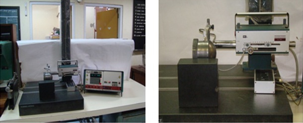
Range: 0-200mm (linear)
Roughness value capability: 0.01 to 200 microns
Measurement of roughness, waviness and other parameters as per ISO/DIN standard.

It measures Total Mass Loss, Collected Volatile Condensable Material confirming to Test standard: ESA-PSS-01-702 and ASTM-E-595 ,TML < 1.0%, CVCM < 0.10%
Test material/ sample requirements: (min) 300mg, bead in cured/dried form of size: (max) 7mm diameter or square made from polymeric materials. up to TML less than 20.0%,CVCM less than 0.01%

RF Frequency: DC - 67 GHz
Temperature Limits: -20 to +125 deg C
Wafer diameter: Up to 6 inch
Die size (min): 0.7mm x 0.7mm x 0.1mm
Probe configuration & Pitch: GS,SG,GSG; 100,150,200 microns

This imaging facility is useful for non-destructive internal visual inspection of components. The system has capability of 10 micron resolution. Object size of 30 mm x 30 mm can be inspected.
VLSI Tester has per pin architecture, 512 digital I/O pins with 100 MHz data rate, 4 source and capture analog pins having 15 MHz bandwidth, 20 channels 0-30V DC power supply and 4 channels 0-75V power supply.

Resistance: 0.01 mΩ to 2 GΩ
Capacitance: 1.0 pF to 1.0F
Inductance: 0.1 nH to 2.0kH
Dissipation Factor: 0.00001 to 1000
Probe Size : Diameter : 0.9 mm
Length : 1.0 meter
Defect size measurement & recording. Video & still photograph for defect library.
Transmission & Reflection parameter measurements ( s parameters): 10 MHz to 40 GHz
Spurious, Harmonics & IMD measurements: 10 MHz to 110 GHz
RF power & frequency measurements: 10 MHz to 110 GHz
Noise figure measurements: 10 MHz to 110 GHz
Phase noise measurements: 10 MHz to 13 GHz
If you have any test facility requirements at SAC, kindly register on following link:
https://www.inspace.gov.in/